2011 – Worldwide semiconductor capital equipment spending is on track to reach $44.8 billion in 2011, a 10.2 per cent increase from 2010 spending of $40.6 billion, according to Gartner, Inc. However, analysts warned that a looming semiconductor inventory correction, combined with oversupply in foundry, will lead to a slight spending decline in 2012.
“Capital spending and the equipment picture have changed little since our last forecast in the first quarter of 2011, in spite of the disastrous earthquake in Japan, which threatened to disrupt the electronics supply chain,” said Klaus Rinnen, managing vice president at Gartner. “Thanks to Herculean efforts by Japanese vendors, the effects of the quake were minimised.”
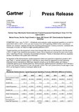
All segments of the semiconductor capital equipment market are expected to experience growth in 2011 (see Table 1). Gartner analysts said 2011 spending is being driven by aggressive foundry spending, integrated device manufacturer (IDM) logic capacity ramping up at the leading edge, and memory companies gearing up for double patterning. Semiconductor capital equipment spending in 2012 will see a 2.6 per cent decline, followed by 8.9 per cent growth in 2013. The next cyclical decline should begin in late 2013, as the impact of memory oversupply takes its toll.
As semiconductor growth continues, worldwide wafer fab equipment (WFE) revenue is expected to grow 11.7 per cent in 2011. Intel, foundry and NAND spending will drive the need for leading-edge equipment, thus benefiting immersion lithography, etch, and certain segments in deposition involved in double patterning and critical leading-edge logic processes.
Worldwide packaging and assembly equipment (PAE) revenue is expected to experience the smallest growth in 2011 at 3.6 per cent. Back-end manufacturers realised sizable growth in 2010, but the market began to slow in the fourth quarter of last year. Orders have softened some as supply comes in line with demand. For back-end process providers- capital expenditures (capex), 3D packaging and copper wire bonding for lower-cost solutions are currently a major focus. Most major tool segments will see growth in 2011, but advanced tooling should outperform the general market this year.
In 2011, the worldwide automated test equipment (ATE) market is expected to grow about 6.9 per cent. Gartner-s 2011 growth expectations are driven by the continued demand from system on a chip (SoC) and the advanced radio frequency (RF) segments of the market. Memory ATE will likely pull back in 2011 as DRAM capex softens. However, NAND testing platforms should remain strong this year.
This research is produced by Gartner-s Semiconductor Manufacturing program. This research program, which is part of the overall semiconductor research group, provides a comprehensive view of the entire semiconductor industry, from manufacturing to device and application market trends. More information on Gartner-s semiconductor research can be found in the Gartner Semiconductor Manufacturing Focus Area at http://www.gartner.com/it/products/research/asset_129175_2395.jsp.
Gartner, Inc. (NYSE: IT) is the world-s leading information technology research and advisory company. Gartner delivers the technology-related insight necessary for its clients to make the right decisions, every day. From CIOs and senior IT leaders in corporations and government agencies, to business leaders in high-tech and telecom enterprises and professional services firms, to technology investors, Gartner is a valuable partner to 60,000 clients in 11,500 distinct organizations. Through the resources of Gartner Research, Gartner Executive Programs, Gartner Consulting and Gartner Events, Gartner works with every client to research, analyze and interpret the business of IT within the context of their individual role. Founded in 1979, Gartner is headquartered in Stamford, Connecticut, U.S.A., and has 4,500 associates, including 1,250 research analysts and consultants, and clients in 85 countries. For more information, visit www.gartner.com.


You must be logged in to post a comment Login